High Frequency PCBs
Microwave Circuit Board
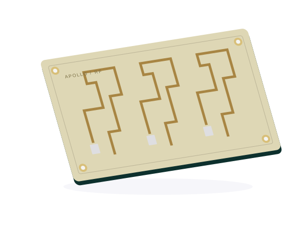
A microwave circuit board example. Bring material references, line geometry and the intended operating conditions.
- Material direction
- RF material — subject to design review
- Project focus
- Signal requirements & critical geometry
- Manufacturing basis
- Current drawings & engineering review
Product overview
Designed into
your next product.
Connect the signal requirements to material references, layer arrangement and critical routing. Identify the conditions that must be preserved in manufacturing.
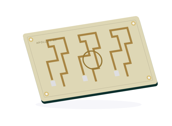
Keep critical signal paths in view.
Bring the proposed materials and stack-up into the review with line geometry, connector details and test expectations. Reference material data and the intended operating conditions together.
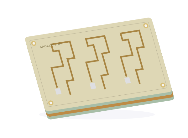
Product type illustration. Materials, construction and final specifications are confirmed for your project.
Application considerations
- RF circuit design
- Signal-sensitive interconnections
- Microwave electronic design
Product specifications
Define the details.
Set the manufacturing brief.
Start with the information already defined in your design. Bring open requirements to the engineering review.
- Product
- Microwave Circuit Board
- Product family
- High Frequency PCBs
- Material direction
- RF material — subject to design review
- Construction
- Critical geometry · Signal requirements
- Board geometry
- Outline, dimensions and mounting — per current drawing
- Copper & surface finish
- Requirements to be confirmed in the fabrication brief
- Signal & impedance requirements
- Operating requirements, impedance targets and critical routing
- Inspection & acceptance
- Inspection method and acceptance criteria agreed per project
Engineering review
Connect the board
to the build.
Bring the proposed materials and stack-up into the review with line geometry, connector details and test expectations. Reference material data and the intended operating conditions together.

Material references and intended use
Connect the current revision and requirements to this review point. Confirm the agreed manufacturing input before proceeding.
Line geometry and impedance targets
Connect the current revision and requirements to this review point. Confirm the agreed manufacturing input before proceeding.
Finish, connectors and test brief
Connect the current revision and requirements to this review point. Confirm the agreed manufacturing input before proceeding.
Project files
Bring your design.
We’ll discuss the next step.
Gerber files, proposed stack-up, material references and signal requirements.
Prepare a Product Enquiry- 01
Current design files
Gerber files, drill data and fabrication drawing with the current revision.
- 02
Materials & interfaces
Operating requirements, impedance targets and critical routing
- 03
Assembly information
BOM, placement data and assembly drawings when assembly is part of your enquiry.
- 04
Quantity & acceptance
Project stage, quantity, target timing and inspection or test requirements.